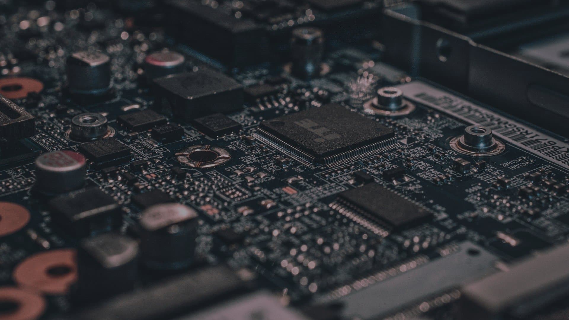
Industries - Electronics
Electronics manufacturing demands inspection accuracy at the micron level across components that are too small and too numerous for reliable human evaluation. Solder joint quality, component placement accuracy, wire bond integrity, and surface mount defects must be verified at speeds that match automated assembly equipment. ConductVision's technology can provide high-resolution visual inspection models trained specifically for electronics manufacturing environments, including PCB assembly, semiconductor packaging, and final product verification. Cleanroom monitoring and ESD compliance tracking can provide additional operational oversight for sensitive production environments.
The challenge
Surface mount components are shrinking to 01005 packages (0.4 x 0.2 mm) that are invisible to unaided human inspection. Solder defects like cold joints, bridging, and insufficient wetting have distinct visual signatures but occur across thousands of joints per board. False reject rates from rule-based AOI systems waste significant operator time on phantom defects.
Our solution
ConductVision can deploy deep learning inspection models that achieve higher defect detection rates with significantly lower false reject rates compared to traditional AOI rule sets. Models can adapt to new component types through transfer learning, reducing new product introduction inspection setup from weeks to days.
Capabilities - AI detection for electronics
Purpose-built detection models that address the specific challenges of electronics.
- People Detection. Real-time occupancy intelligence from any camera feed — available for deployment at any scale.
- Environmental Monitoring. Water levels, flood risk, vegetation health, and erosion — visual intelligence born from ConductScience's environmental research heritage — available for deployment.
- Behavioral Analytics. Loitering, aggression, crowd surges, and abandoned objects — anomaly detection grounded in behavioral science — available for deployment.
- Quality & Defect Inspection. Detect surface defects, dimensional deviations, and assembly errors at production speed — available for deployment on any line.
Use cases
How organizations in electronics are using ConductVision.
Solder Joint Inspection
High-magnification cameras can evaluate solder joint quality on SMT and through-hole assemblies, detecting cold joints, bridging, tombstoning, and insufficient wetting. Deep learning models can distinguish true defects from acceptable process variation, reducing false rejects.
Component Placement Verification
Post-placement cameras can verify component presence, correct orientation, polarity markings, and positional accuracy against design data. Missing or misaligned components can be flagged before reflow, preventing costly post-reflow rework.
Wire Bond and Die Attach Inspection
Semiconductor packaging inspection can verify wire bond loop height, tail length, ball placement, and die attach void coverage. Defects can be classified and tracked to specific bonder heads or tool settings for process correction.
Cleanroom Monitoring
Cameras can monitor cleanroom gowning compliance, particle-generating activities, and door seal integrity. Personnel traffic patterns can be analyzed to identify contamination risk behaviors and optimize cleanroom layout and protocols.
ESD Compliance Tracking
Detection models can verify wrist strap usage, ESD smock wearing, and proper grounding practices at workstations. Compliance events can be logged for quality system auditing and correlated with field failure data for root-cause analysis.
Exploring AI vision for electronics?
Tell us about your environment and challenges. We will show you exactly what our technology can detect and measure.
Integration ecosystem
ConductVision integrates with the tools and systems already used in electronics.
- AOI Systems (Koh Young, CyberOptics)
- MES (Manufacturing Execution Systems)
- Pick-and-Place Machine Controllers
- SPC/Statistical Process Control Platforms
- Traceability Systems (Aegis, Valor)
Related industries
All capabilities
Ready to explore what AI vision can do for you?
Contact us
- Headquarters
ConductScience Inc.
5250 Old Orchard Rd Suite 300
Skokie, IL 60077
+1 (847) 983-3672 - Sales & Support
info@conductscience.com
Mon – Fri, 9 AM – 5 PM EST